PCB stack-up is an important factor in determining the EMC performance of a product. A good stack-up can be very effective in reducing radiation from the loops on the PCB, as well as the cables attached to the board.
Four factors are important with respect to board stack-up considerations:
1. The number of layers,
2. The number and types of planes (power and/or ground) used,
3. The ordering or sequence of the layers, and
4. The spacing between the layers.
Usually not much consideration is given except as to the number of layers. In many cases the other three factors are of equal importance. In deciding on the number of layers, the following should be considered:
1. The number of signals to be routed and cost,
2. Frequency
3. Will the product have to meet Class A or Class B emission requirements?
Often only the first item is considered. In reality all the items are of critical importance and should be considered equally. If an optimum design is to be achieved in the minimum amount of time and at the lowest cost, the last item can be especially important and should not be ignored.
The above paragraph should not be construed to mean that you can’t do a good EMC design on a four- or six-layer board, because you can. It only indicates that all the objectives cannot be met simultaneously and some compromise will be necessary. Since all the desired EMC objectives can be met with an eight-layer board, there is no reason for using more than eight layers other than to accommodate additional signal routing layers.
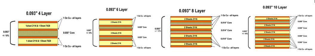
The standard pooling thickness for multilayer PCBs is 1.55mm. Here are some examples of multilayer PCB stack up.