HDI PCBs is the latest technologies available to increase the functionality of PCBs using the same or less amount of area. This advanced PCB technology is driven by the miniaturization of components and semiconductor packages that supports advanced features in revolutionary new products. This includes touch screen computing, 4G network communications and military applications.
HDI PCBs are characterized by high-density attributes including laser micro vias, fine lines and high performance thin materials. This increased density enables more functions per unit area. Higher technology HDI PCBs have multiple layers of copper filled stacked micro vias (Advanced HDI PCBs) which creates a structure that enables even more complex interconnections. These very complex structures provide the necessary routing solutions for today’s large pin-count chips utilized in mobile devices and other high technology products.
HDI Benefits
By using HDI technology, designers now have the option to place more components on both sides of the raw PCB. Multiple via processes, including via in pad and blind via technology, allow designers more PCB real estate to place components that are smaller even closer together. Decreased component size and pitch allow for more I/O in smaller geometries. This means faster transmission of signals and a significant reduction in signal loss and crossing delays.
HDI structures
1) 1+N+1 – PCBs contain 1 “build-up” of high-density interconnection layers.
2) i+N+i (i≥2) – PCBs contain 2 or more “build-up” of high density interconnection layers. Micro vias on different layers can be staggered or stacked. Copper filled stacked micro via structures are commonly seen in challenging designs.
3) Any Layer HDI – All the layers of a PCB are high density interconnection layers which allows the conductors on any layer of the PCB to be interconnected freely with copper filled stacked micro via structures (“any layer via”). This provides a reliable interconnect solution for highly complex large pin-count devices, such as CPU and GPU chips utilized on handheld and mobile devices.
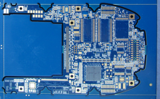
HDI PCB for rugged PC
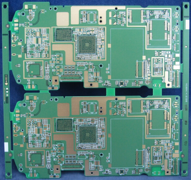
HDI PCB for tablet