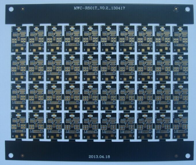
If you are having PCBs produced for the first time, you would have many doubts to choose the substrate material, fire rating, solder mask, overlay inks, board thickness, copper thickness, through-hole plating, penalization, and so on. One of the most important decisions is the selection of surface finish.
In this chapter, we would introduce the ENIG in surface finish. ENIG stands for “Electroless Nickel Im mersion Gold”. It consists of an underlying layer o
 f nickel with a thin layer of gold over the top. The gold layer is very thin and not intended to provide the main structure of the track, it just acts as a protective coating for the nickel to prevent it tarnishing before it’s soldered. Gold is extremely resistant to corrosion so ENIG has several good points: it can be touched with bare fingers without tarnishing, has a very long shelf life and the pads / tracks are very flat and square-edged – something that can be important for fine-pitch surface-mount parts.
One one bad aspect to ENIG is that it takes a bit more solder to complete a joint because the surface hasn’t yet been pre-tinned, and because there isn’t an existing layer of solder to melt against the iron and increase the initial contact area (hence increasing the rate of heat transfer) it can take an extra second or so to get the joint hot. You really need to make sure your iron has good contact with the joint to make sure enough heat is transferred to the track and the component lead.

