The benefits of via-in-pad designs are well documented. From reduction of inductance to increased density, via-in-pad has become an essential tool for designers when navigating the routing challenges of fine pitch array packages. There are some applications that may require, or seem to require, via in pad. Here are a few examples of why you might need to use via in pad:
> If there is not enough space on the board.
> It can help with thermal management.
> Trace routing may be easier with via in pad.
> High frequency designs benefit from the shortest possible routing to bypass capacitors, which may indicate via in pad.
Here are some methods you can try when using via in pad:
> Plug the via and then plate copper over it. This is our favorite option. It will give you all of the benefits of via in pad without causing problems in assembly.
> Use a micro-via that only goes through one layer of the board. Although this may be an okay option, the solder can still wander down into the via, leaving voids.
> Cap the underside of the board with solder mask. This is our least favorite option because sometimes the cap can pop open, and the void may be big enough to still pull too much of the solder off of the pad.
However, there are disadvantages when implementing via-in-pad technology. The process may increase the PCB cost. The reason is that the via-in-pad technique requires both additional process steps and extra materials. Added costs are found in both the extra materials used, including epoxy or metal based via fill materials and copper cap plating processes, as well as added process steps like vacuum via fill, curing, planarization and secondary plating operations. There is also the general challenge that results from producing a higher density PCB.
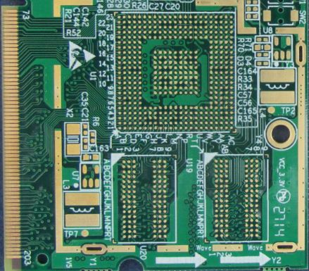
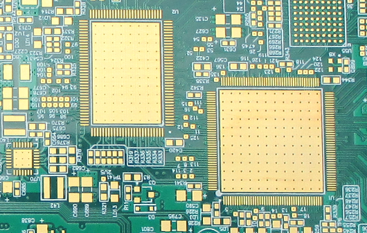
At Pandawill Circuits, Via in pad is a standard technology available. Here are some of the PCB boards with via in pad for your reference.